


Features
Commercial: 0 ~ 70℃
Extended: -5 ~ +85℃
Applications
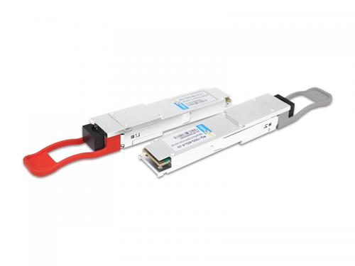
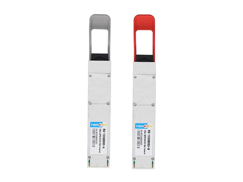
100Gb/s QSFP28 ZR4 BIDI Single fiber 80km Transceiver
RQ-100GBD80-A/RQ-100GBD80-B

FIBERWDM’ RQ-100GBD80-A/RQ-100GBD80-B is designed for 100G 80km single fiber optical communication applications. This module contains 4-lane optical transmitter, 4-lane optical receiver and module management block including 2 wire serial inter-face. The optical signals are multiplexed to a single-mode fiber through an industry standard LC connector. A block diagram is shown in Figure 1.
Electrical Characteristics
The following electrical characteristics are defined over the Recommended Operating Environment unless otherwise specified.
|
Parameter |
Symbol |
Min. |
Typ. |
Max |
Unit |
Notes |
|
Power Consumption |
p |
|
|
5.5 |
W |
|
|
Supply Current |
Icc |
|
|
1585 |
mA |
|
|
|
||||||
|
Input differential impedance |
Rin |
|
100 |
|
Ω |
|
|
Differential Termination Mismatch |
|
|
|
10 |
% |
|
|
Differential Data Input Amplitude |
Vin, PP |
180 |
|
1000 |
mV |
|
|
LPMode, Reset and ModSelL |
VIL |
-0.3 |
|
0.8 |
V |
|
|
VIH |
2 |
|
Vcc+0.3 |
V |
|
|
|
Receiver |
||||||
|
Differential Data Output Amplitude |
Vout, PP |
350 |
|
900 |
mV |
|
|
Differential Termination Mismatch |
|
|
|
10 |
% |
|
|
Transition Time, 20 to 80% |
|
9.5 |
|
|
ps |
|
|
ModPrsL and IntL |
VOL |
0 |
|
0.4 |
V |
|
|
VOH |
Vcc-0.5 |
|
Vcc+0.3 |
V |
|
|
Optical Characteristics
The following optical characteristics are defined over the Recommended Operating Environment unless otherwise specified.
|
Parameter |
Symbol |
Min. |
Typical |
Max |
Unit |
Notes |
||
|
Transmitter |
||||||||
|
Lane wavelength(range) |
RQ-100GBD80-A |
L0 |
1272.55 |
1273.55 |
1274.54 |
nm |
|
|
|
L1 |
1276.89 |
1277.89 |
1278.89 |
nm |
|
|||
|
L2 |
1281.25 |
1282.26 |
1283.27 |
nm |
|
|||
|
L3 |
1285.65 |
1286.66 |
1287.68 |
nm |
|
|||
|
RQ-100GBD80-B |
L4 |
1294.53 |
1295.56 |
1296.59 |
nm |
|
||
|
L5 |
1299.02 |
1300.05 |
1301.09 |
nm |
|
|||
|
L6 |
1303.54 |
1304.58 |
1305.63 |
nm |
|
|||
|
L7 |
1308.09 |
1309.14 |
1310.09 |
nm |
|
|||
|
Signaling rate, each lane |
|
|
25.78125 |
28.05 |
Gb/s |
|
||
|
Side-mode suppression ratio |
SMSR |
30 |
|
|
|
|
||
|
Total launch power |
PT |
8.0 |
|
10.5 |
dBm |
|
||
|
Average launch power, each lane |
Pavg |
2.0 |
|
4.5 |
dBm |
|
||
|
Extinction Ratio |
ER |
6.0 |
|
|
dB |
|
||
|
Difference in Launch Power between any Two Lanes (OMA) |
Ptx,diff |
|
|
3.6 |
dB |
|
||
|
Average launch power of OFF transmitter, each lane |
Poff |
|
|
-30 |
dBm |
|
||
|
Transmitter reflectance |
RT |
|
|
-12 |
dB |
|
||
|
RIN20OMA |
RIN |
|
|
-130 |
dB/Hz |
|
||
|
Optical Return Loss Tolerance |
TOL |
|
|
20 |
dB |
|
||
|
Transmitter eye mask {X1, X2, X3, Y1, Y2, Y3} |
|
{0.25, 0.4, 0.45, 0.25, 0.28, 0.4} |
|
|
||||
|
Receiver |
||||||||
|
Lane wavelength(range) |
RQ-100GBD80-A
|
L0 |
1294.53 |
1295.56 |
1296.59 |
nm |
|
|
|
L1 |
1299.02 |
1300.05 |
1301.09 |
nm |
|
|||
|
L2 |
1303.54 |
1304.58 |
1305.63 |
nm |
|
|||
|
L3 |
1308.09 |
1309.14 |
1310.09 |
nm |
|
|||
|
RQ-100GBD80-B |
L4 |
1272.55 |
1273.55 |
1274.54 |
nm |
|
||
|
L5 |
1276.89 |
1277.89 |
1278.89 |
nm |
|
|||
|
L6 |
1281.25 |
1282.26 |
1283.27 |
nm |
|
|||
|
L7 |
1285.65 |
1286.66 |
1287.68 |
nm |
|
|||
|
Signaling rate, each lane |
|
|
25.78125 |
28.05 |
Gb/s |
|
||
|
Average Receive Power, each Lane |
|
-30 |
|
-7 |
dBm |
|
||
|
Receive Power (OMA), each Lane |
|
|
|
-7 |
dBm |
|
||
|
Receiver reflectance |
|
|
|
-26 |
dB |
|
||
|
Receiver sensitivity Average, each lane |
SEN1 |
|
|
-22 |
dBm |
1 |
||
|
SEN2 |
|
|
-21 |
dBm |
2 |
|||
|
SEN3 |
|
|
-28 |
dBm |
3 |
|||
|
SEN4 |
|
|
-27 |
dBm |
4 |
|||
|
LOS Assert |
LOSA |
-40 |
|
|
dBm |
|
||
|
LOS Deassert |
LOSD |
|
|
-29 |
dBm |
|
||
|
LOS Hysteresis |
LOSH |
0.5 |
|
|
dB |
|
||
Notes:
1. Measured @25.78125Gbps, ER=8.2dB, BER=<1E-12, PRBS=2³¹-1 NRZ
2. Measured @28.05Gbps, ER=8.2dB, BER=<1E-12, PRBS=2³¹-1 NRZ
3. Measured @25.78125Gbps, ER=8.2dB, BER=<5E-5, PRBS=2³¹-1 NRZ
4. Measured @28.05Gbps, ER=8.2dB, BER=<5E-5, PRBS=2³¹-1 NRZ
Digital Diagnostic Functions
The following digital diagnostic characteristics are defined over the normal operating conditions unless otherwise specified.
|
Parameter |
Symbol |
Min. |
Max |
Unit |
Range |
|
Temperature monitor absolute error |
DMI_ Temp |
-3 |
3 |
℃ |
-40~85C |
|
Supply voltage monitor absolute error |
DMI _VCC |
-3 |
3 |
% |
0~Vcc |
|
RX power monitor absolute error |
DMI_RX |
-3 |
3 |
dB |
-7~-30dBm |
|
Bias current monitor error |
DMI_ bias |
-10 |
10 |
% |
0~120mA |
|
TX power monitor absolute error |
DMI_TX |
-3 |
3 |
dB |
2~4.5dBm |
Absolute Maximum Ratings
It has to be noted that the operation in excess of any individual absolute maximum ratings might cause permanent damage to this module.
|
Parameter |
Symbol |
Min |
Max |
Unit |
Notes |
|
Storage Temperature |
TS |
-40 |
85 |
℃ |
|
|
Power Supply Voltage |
VCC |
-0.3 |
4.0 |
V |
|
|
Relative Humidity (non-condensation) |
RH |
15 |
85 |
% |
|
|
Damage Threshold |
THd |
6.5 |
|
dBm |
|
Recommended Operating Conditions
|
Parameter |
Symbol |
Min |
Typical |
Max |
Unit |
Notes |
|
Operating Case Temperature |
TOP |
0 |
|
70 |
℃ |
Commercial |
|
-5 |
|
85 |
℃ |
Extended |
||
|
-40 |
|
85 |
℃ |
Industrial |
||
|
Power Supply Voltage |
VCC |
3.135 |
3.3 |
3.465 |
V |
|
|
Data Rate, each Lane |
|
|
25.78125 |
28.05 |
Gb/s |
|
|
Control Input Voltage High |
|
2 |
|
Vcc |
V |
|
|
Control Input Voltage Low |
|
0 |
|
0.8 |
V |
|
|
Link Distance (SMF) |
D |
|
|
80 |
km |
1 |
Notes:
1. Depending on actual fiber loss/km (link distance specified is for fiber insertion loss of 0.35dB/km)
ModSeIL
The ModSelL is an input pin. When held low by the host, the module responds to 2-wire serial communication commands. The ModSelL allows the use of multiple modules on a single 2-wire interface bus. When the ModSelL is "High", the module shall not respond to or acknowledge any 2-wire interface communication from the host. ModSelL signal input node shall be biased to the "High" state in the module.
In order to avoid conflicts, the host system shall not attempt 2-wire interface communications within the ModSelL de-assert time after any modules are deselected. Similarly, the host shall wait at least for the period of the ModSelL assert time before communicating with the newly selected module. The assertion and de-asserting periods of different modules may overlap as long as the above timing requirements are met.
ResetL:
The ResetL pin shall be pulled to Vcc in the module. A low level on the ResetL pin for longer than the minimum pulse length (t_Reset_init) initiates a complete module reset, returning all user module settings to their default state. Module Reset Assert Time (t_init) starts on the rising edge after the low level on the ResetL pin is released. During the execution of a reset (t_init) the host shall disregard all status bits until the module indicates a completion of the reset interrupt. The module indicates this by asserting "low" an IntL signal with the Data Not_Ready bit negated. Note that on power up (including hot insertion) the module should post this completion of reset interrupt without requiring a reset.
LPMode:
LPMode: The LPMode pin shall be pulled up to Vcc in the module. The pin is a hardware control used to put modules into a low power mode when high. By using the LPMode pin and a combination of the Power override, Power_set and High_Power_Class_Enable software control bits (Address A0h, byte 93 bits 0,1,2).
ModPrsL:
ModPrsL is pulled up to Vcc_Host on the host board and grounded in the module. The ModPrsL is asserted "Low" when inserted and deasserted "High" when the module is physically absent from the host connector.
IntL:
IntL is an output pin. When IntL is "Low", it indicates a possible module operational fault or a status critical to the host system. The host identifies the source of the interrupt using the 2-wire serial interface. The IntL pin is an open collector output and shall be pulled to host supply voltage on the host board. The INTL pin is deasserted "High" after completion of reset, when byte 2 bit 0 (Data Not Ready) is read with a value of '0' and the flag field is read .
Pin Assignment and Pin Description
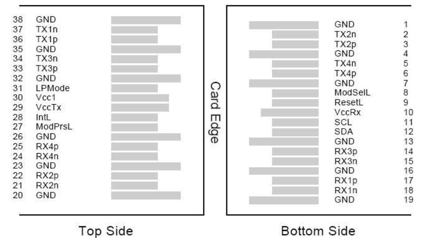
Figure1. Diagram of host board connector block pin numbers and names
|
Pin |
Symbol |
Name/Description |
Notes |
|
1 |
GND |
Transmitter Ground (Common with Receiver Ground) |
1 |
|
2 |
Tx2n |
Transmitter Inverted Data Input |
|
|
3 |
Tx2p |
Transmitter Non-Inverted Data output |
|
|
4 |
GND |
Transmitter Ground (Common with Receiver Ground) |
1 |
|
5 |
Tx4n |
Transmitter Inverted Data Input |
|
|
6 |
Tx4p |
Transmitter Non-Inverted Data output |
|
|
7 |
GND |
Transmitter Ground (Common with Receiver Ground) |
1 |
|
8 |
ModSelL |
Module Select |
|
|
9 |
ResetL |
Module Reset |
|
|
10 |
VccRx |
3.3V Power Supply Receiver |
2 |
|
11 |
SCL |
2-Wire serial Interface Clock |
|
|
12 |
SDA |
2-Wire serial Interface Data |
|
|
13 |
GND |
Transmitter Ground (Common with Receiver Ground) |
|
|
14 |
Rx3p |
Receiver Non-Inverted Data Output |
|
|
15 |
Rx3n |
Receiver Inverted Data Output |
|
|
16 |
GND |
Transmitter Ground (Common with Receiver Ground) |
1 |
|
17 |
Rx1p |
Receiver Non-Inverted Data Output |
|
|
18 |
Rx1n |
Receiver Inverted Data Output |
|
|
19 |
GND |
Transmitter Ground (Common with Receiver Ground) |
1 |
|
20 |
GND |
Transmitter Ground (Common with Receiver Ground) |
1 |
|
21 |
Rx2n |
Receiver Inverted Data Output |
|
|
22 |
Rx2p |
Receiver Non-Inverted Data Output |
|
|
23 |
GND |
Transmitter Ground (Common with Receiver Ground) |
1 |
|
24 |
Rx4n |
Receiver Inverted Data Output |
1 |
|
25 |
Rx4p |
Receiver Non-Inverted Data Output |
|
|
26 |
GND |
Transmitter Ground (Common with Receiver Ground) |
1 |
|
27 |
ModPrsl |
Module Present |
|
|
28 |
IntL |
Interrupt |
|
|
29 |
VccTx |
3.3V power supply transmitter |
2 |
|
30 |
Vcc1 |
3.3V power supply |
2 |
|
31 |
LPMode |
Low Power Mode |
|
|
32 |
GND |
Transmitter Ground (Common with Receiver Ground) |
1 |
|
33 |
Tx3p |
Transmitter Non-Inverted Data Input |
|
|
34 |
Tx3n |
Transmitter Inverted Data Output |
|
|
35 |
GND |
Transmitter Ground (Common with Receiver Ground) |
1 |
|
36 |
Tx1p |
Transmitter Non-Inverted Data Input |
|
|
37 |
Tx1n |
Transmitter Inverted Data Output |
|
|
38 |
GND |
Transmitter Ground (Common with Receiver Ground) |
1 |
Notes:
1. GND is the symbol for signal and supply (power) common for QSFP28 modules. All are common within the QSFP28 module and all module voltages are referenced to this potential unless otherwise noted. Connect these directly to the host board signal common ground plane.
2. VccRx, Vcc1 and VccTx are the receiving and transmission power suppliers and shall be applied concurrently. Recommended host board power supply filtering is shown below. Vcc Rx, Vcc1 and Vcc Tx may be internally connected within the QSFP28 transceiver module in any combination. The connector pins are each rated for a maximum current of 1000mA.
Mechanical Dimensions
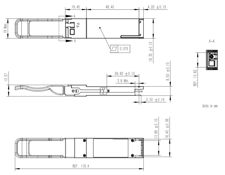
Figure2. Mechanical Outline
Order information
|
Part Number |
Product Description |
|
RQ-100GBD80-A |
100G QSFP28 BIDI Transceiver, TX1273.55/1277.89/1282.26/1286.66nm/ RX1295.56/1300.05/1304.58/1309.14nm, Simplex LC, 80km, 0~+70°C, with DDM |
|
RQ-100GBD80-B |
100G QSFP28 BIDI Transceiver, TX1295.56/1300.05/1304.58/1309.14nm/ RX1273.55/1277.89/1282.26/1286.66nm, Simplex LC, 80km, 0~+70°C, with DDM |
Want to know about this product?
If you are interested in our products and want to know more details,please leave a message here,we will reply you as soon as we can.
 100G QSFP28 SR4 100m 850nm MPO Optical Transceiver
 100G QSFP28 CWDM4 2km LC Optical Transceiver
 100G QSFP28 LR4 1310nm 10km LC Optical Transceiver
 100G QSFP28 ER4 40Km 1310nm LC Optical Transceiver
 100Gb QSFP28 ZR4 80Km 1310nm LC Optical Transceiver
 100G DWDM QSFP28 Dual CS Connector PAM4 Transceiver
 100GBASE-SR Bi-Directional QSFP28 850/900nm 100m DOM LC MMF Optical Transceiver Module
 100GBASE-LR Bi-Directional QSFP28 1280/1310nm 20km LC SM Optical Transceiver Module

Address : Third floor, Building A, 118 Creative Park, No. 241 Bussiness Road, Huadu, Guanzhou, PRC
Tel : +86 15989256178
Whatsapp : +86 15914235380
Email : sales@fiberwdm.com
Skype : 15914235380


